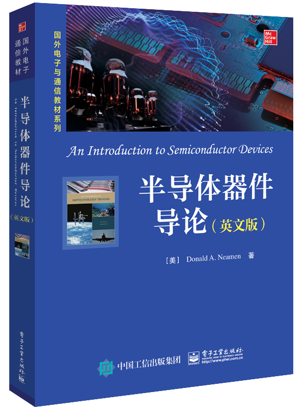
半导体器件导论(英文版)
丛 书 名:
国外电子与通信教材系列
作 译 者:Donald A. Neamen(唐纳德 • A. 尼曼)
出 版 日 期:2023-03-01
书 代 号:G0448970
I S B N:9787121448973
图书简介:
本书适合作为集成电路、微电子、电子科学与技术等专业高年级本科生和研究生学习半导体器件物理的双语教学教材,内容涵盖了量子力学、固体物理、半导体物理和半导体器件的全部内容。全书在介绍学习器件物理所必需的基础理论之后,重点讨论了pn结、金属–半导体接触、MOS场效应晶体管和双极型晶体管的工作原理和基本特性。最后论述了结型场效应晶体管、晶闸管、MEMS和半导体光电器件的相关内容。本书提供了丰富的习题和自测题,并给出了大量的分析或设计实例,有助于读者对基本理论和概念的理解。
-
配 套 资 源
本书资源
本书暂无资源 -
图 书 内 容
内容简介
本书适合作为集成电路、微电子、电子科学与技术等专业高年级本科生和研究生学习半导体器件物理的双语教学教材,内容涵盖了量子力学、固体物理、半导体物理和半导体器件的全部内容。全书在介绍学习器件物理所必需的基础理论之后,重点讨论了pn结、金属–半导体接触、MOS场效应晶体管和双极型晶体管的工作原理和基本特性。最后论述了结型场效应晶体管、晶闸管、MEMS和半导体光电器件的相关内容。本书提供了丰富的习题和自测题,并给出了大量的分析或设计实例,有助于读者对基本理论和概念的理解。图书详情
ISBN:9787121448973开 本:16(185*260)页 数:692字 数:1439本书目录
CHAPTER 1 The Crystal Structure of Solids 固体的晶体结构 1.0 PREVIEW 概览 1.1 SEMICONDUCTOR MATERIALS 半导体材料 1.2 TYPES OF SOLIDS 固体类型 1.3 SPACE LATTICES 空间点阵 1.3.1 Primitive and Unit Cell 原胞与晶胞 1.3.2 Basic Crystal Structures 基本晶体结构 1.3.3 Crystal Planes and Miller Indices 晶面和米勒指数 1.3.4 The Diamond Structure 金刚石结构 1.4 ATOMIC BONDING 原子价键 1.5 IMPERFECTIONS AND IMPURITIES IN SOLIDS 固体中的缺陷和杂质 1.5.1 Imperfections in Solids 固体缺陷 1.5.2 Impurities in Solids 固体中的杂质 Σ1.6 GROWTH OF SEMICONDUCTOR MATERIALS 半导体材料生长 1.6.1 Growth from a Melt 熔体生长 1.6.2 Epitaxial Growth 外延生长 Σ1.7 DEVICE FABRICATION TECHNIQUES: OXIDATION 器件制备技术:氧化 1.8 SUMMARY 小结 PROBLEMS 习题 CHAPTER 2 Theory of Solids 固体理论 2.0 PREVIEW 概览 2.1 PRINCIPLES OF QUANTUM MECHANICS 量子力学的基本原理 2.1.1 Energy Quanta 能量子 2.1.2 Wave-Particle Duality Principle 波粒二象性 2.2 ENERGY QUANTIZATION AND PROBABILITY CONCEPTS 能量量子化和概率 2.2.1 Physical Meaning of the Wave Function 波函数的物理意义 2.2.2 The One-Electron Atom 单电子原子 2.2.3 Periodic Table 元素周期表 2.3 ENERGY-BAND THEORY 能带理论 2.3.1 Formation of Energy Bands 能带的形成 2.3.2 The Energy Band and the Bond Model 能带与价键模型 2.3.3 Charge Carriers—Electrons and Holes 载流子——电子和空穴 2.3.4 Effective Mass 有效质量 2.3.5 Metals, Insulators, and Semiconductors 金属、 绝缘体和半导体 2.3.6 The k-Space Diagram k 空间能带图 2.4 DENSITY OF STATES FUNCTION 态密度函数 2.5 STATISTICAL MECHANICS 统计力学 2.5.1 Statistical Laws 统计规律 2.5.2 The Fermi-Dirac Distribution Function and the Fermi Energy 费米-狄拉克分布和费米能级 2.5.3 Maxwell-Boltzmann Approximation 麦克斯韦-玻尔兹曼近似 2.6 SUMMARY 小结 PROBLEMS 习题 CHAPTER 3 The Semiconductor in Equilibrium 平衡半导体 3.0 PREVIEW 概览 3.1 CHARGE CARRIERS IN SEMICONDUCTORS 半导体中的载流子 3.1.1 Equilibrium Distribution of Electrons and Holes 电子和空穴的平衡分布 3.1.2 The n0 and p0 Equations 平衡电子和空穴浓度方程 3.1.3 The Intrinsic Carrier Concentration 本征载流子浓度 3.1.4 The Intrinsic Fermi-Level Position 本征费米能级的位置 3.2 DOPANT ATOMS AND ENERGY LEVELS 掺杂原子与能级 3.2.1 Qualitative Description 定性描述 3.2.2 Ionization Energy 电离能 3.2.3 Group III-V Semiconductors III-V族半导体 3.3 CARRIER DISTRIBUTIONS IN THE EXTRINSIC SEMICONDUCTOR 非本征半导体的载流子分布 3.3.1 Equilibrium Distribution of Electrons and Holes 电子和空穴的平衡分布 3.3.2 The n0 p0 Product n0 p0 积 Σ3.3.3 The Fermi-Dirac Integral 费米-狄拉克积分 3.3.4 Degenerate and Nondegenerate Semiconductors 简并与非简并半导体 3.4 STATISTICS OF DONORS AND ACCEPTORS 施主和受主的统计分布 3.4.1 Probability Function 概率分布函数 Σ3.4.2 Complete Ionization and Freeze-Out 完全电离与冻析 3.5 CARRIER CONCENTRATIONS—EFFECTS OF DOPING 载流子浓度——掺杂的影响 3.5.1 Compensated Semiconductors 补偿半导体 3.5.2 Equilibrium Electron and Hole Concentrations 平衡电子和空穴浓度 3.6 POSITION OF FERMI ENERGY LEVEL—EFFECTS OF DOPING AND TEMPERATURE 费米能级的位置——掺杂和温度的影响 3.6.1 Mathematical Derivation 数学推导 3.6.2 Variation of EF with Doping Concentration and Temperature EF 随掺杂浓度和温度的变化 3.6.3 Relevance of the Fermi Energy 费米能级的关联性 Σ3.7 DEVICE FABRICATION TECHNOLOGY: DIFFUSION AND ION IMPLANTATION 器件制备技术:扩散和离子注入 3.7.1 Impurity Atom Diffusion 杂质原子扩散 3.7.2 Impurity Atom Ion Implantation 离子注入 3.8 SUMMARY 小结 PROBLEMS 习题 CHAPTER 4 Carrier Transport and Excess Carrier Phenomena 载流子输运和过剩载流子现象 4.0 PREVIEW 概览 4.1 CARRIER DRIFT 载流子的漂移运动 4.1.1 Drift Current Density 漂移电流密度 4.1.2 Mobility Effects 迁移率 4.1.3 Semiconductor Conductivity and Resistivity 半导体的电导率和电阻率 4.1.4 Velocity Saturation 速度饱和 4.2 CARRIER DIFFUSION 载流子的扩散运动 4.2.1 Diffusion Current Density 扩散电流密度 4.2.2 Total Current Density 总电流密度 4.3 GRADED IMPURITY DISTRIBUTION 渐变杂质分布 4.3.1 Induced Electric Field 感应电场 4.3.2 The Einstein Relation 爱因斯坦关系 4.4 CARRIER GENERATION AND RECOMBINATION 载流子的产生与复合 4.4.1 The Semiconductor in Equilibrium 平衡半导体 4.4.2 Excess Carrier Generation and Recombination 过剩载流子的产生与复合 4.4.3 Generation-Recombination Processes 产生-复合过程 Σ4.5 THE HALL EFFECT 霍尔效应 4.6 SUMMARY 小结 PROBLEMS 习题 CHAPTER 5 The pn Junction and Metal-Semiconductor Contact pn结和金属-半导体接触 5.0 PREVIEW 概览 5.1 BASIC STRUCTURE OF THE PN JUNCTION PN结的基本结构 5.2 THE PN JUNCTION—ZERO APPLIED BIAS 零偏PN结 5.2.1 Built-In Potential Barrier 内建电势 5.2.2 Electric Field 电场 5.2.3 Space Charge Width 空间电荷区宽度 5.3 THE PN JUNCTION—REVERSE APPLIED BIAS 反偏PN结 5.3.1 Space Charge Width and Electric Field 空间电荷区宽度与电场 5.3.2 Junction Capacitance 势垒电容 5.3.3 One-Sided Junctions 单边突变结 5.4 METAL-SEMICONDUCTOR CONTACT—RECTIFYING JUNCTION 金属-半导体接触——整流结 5.4.1 The Schottky Barrier 肖特基势垒结 5.4.2 The Schottky Junction—Reverse Bias 反偏肖特基结 5.5 FORWARD APPLIED BIAS—AN INTRODUCTION 正偏结简介 5.5.1 The pn Junction pn结 5.5.2 The Schottky Barrier Junction 肖特基势垒结 5.5.3 Comparison of the Schottky Diode and the pn Junction Diode 肖特基二极管和pn结二极管的比较 Σ5.6 METAL-SEMICONDUCTOR OHMIC CONTACTS 金属-半导体的欧姆接触 Σ5.7 NONUNIFORMLY DOPED PN JUNCTIONS 非均匀掺杂PN结 5.7.1 Linearly Graded Junctions 线性缓变结 5.7.2 Hyperabrupt Junctions 超突变结 5.8 DEVICE FABRICATION TECHNIQUES: PHOTOLITHOGRAPHY, ETCHING, AND BONDING 器件制备技术:光刻、刻蚀和键合 5.8.1 Photomasks and Photolithography 光学掩膜版和光刻 5.8.2 Etching 刻蚀 5.8.3 Impurity Diffusion or Ion Implantation 杂质扩散或离子注入 5.8.4 Metallization, Bonding, and Packaging 金属化、键合和封装 5.9 SUMMARY 小结 PROBLEMS 习题 CHAPTER 6 Fundamentals of the Metal-Oxide-Semiconductor Field-Effect Transistor MOS场效应晶体管基础 6.0 PREVIEW 概览 6.1 THE MOSFIELD-EFFECT TRANSISTOR ACTION MOS场效应晶体管作用 6.1.1 Basic Principle of Operation 基本工作原理 6.1.2 Modes of Operation 工作模式 6.1.3 Amplification with MOSFETs MOSFET放大 6.2 THE TWO-TERMINAL MOSCAPACITOR 双端 MOS电容 6.2.1 Energy-Band Diagrams and Charge Distributions 能带结构和电荷分布 6.2.2 Depletion Layer Thickness 耗尽层厚度 6.3 POTENTIAL DIFFERENCES IN THE MOSCAPACITOR MOS电容的电势差 6.3.1 Work Function Differences 功函数差 6.3.2 Oxide Charges 氧化层电荷 6.3.3 Flat-Band Voltage 平带电压 6.3.4 Threshold Voltage 阈值电压 Σ6.3.5 Electric Field Profile 电场分布 6.4 CAPACITANCE-VOLTAGE CHARACTERISTICS 电容-电压特性 6.4.1 Ideal C-V Characteristics 理想C-V 特性 Σ6.4.2 Frequency Effects 频率影响 Σ6.4.3 Fixed Oxide and Interface Charge Effects 氧化层固定电荷和界面电荷的影响 6.5 THE BASIC MOSFETOPERATION MOSFET基本工作原理 6.5.1 MOSFETStructures MOSFET结构 6.5.2 Current-Voltage Relationship—Basic Concepts 电流-电压关系——基本概念 Σ6.5.3 Current-Voltage Relationship—Mathematical Derivation 电流-电压关系——数学推导 6.5.4 Substrate Bias Effects 衬底偏置效应 6.6 SMALL-SIGNAL EQUIVALENT CIRCUIT AND FREQUENCY LIMITATION FACTORS 小信号等效电路及频率限制因素 6.6.1 Transconductance 跨导 6.6.2 Small-Signal Equivalent Circuit 小信号等效电路 6.6.3 Frequency Limitation Factors and Cutoff Frequency 频率限制因素与截止频率 Σ6.7 DEVICE FABRICATION TECHNIQUES 器件制备技术 6.7.1 Fabrication of an NMOS Transistor NMOS晶体管的制备 6.7.2 The CMOS Technology CMOS技术 6.8 SUMMARY 小结 PROBLEMS 习题 CHAPTER 7 Metal-Oxide-Semiconductor Field-Effect Transistor: Additional Concepts MOS场效应晶体管的其他概念 7.0 PREVIEW 概览 7.1 MOSFETSCALING MOSFET按比例缩小法则 7.1.1 Constant-Field Scaling 恒电场按比例缩小法则 7.1.2 Threshold Voltage—First Approximation 阈值电压——一级近似 7.1.3 Generalized Scaling 一般按比例缩小法则 7.2 NONIDEAL EFFECTS 非理想效应 7.2.1 Subthreshold Conduction 亚阈值电导 7.2.2 Channel Length Modulation 沟道长度调制效应 7.2.3 Mobility Variation 沟道迁移率变化 7.2.4 Velocity Saturation 速度饱和 7.3 THRESHOLD VOLTAGE MODIFICATIONS 阈值电压修正 7.3.1 Short-Channel Effects 短沟道效应 7.3.2 Narrow-Channel Effects 窄沟道效应 7.3.3 Substrate Bias Effects 衬底偏置效应 7.4 ADDITIONAL ELECTRICAL CHARACTERISTICS 其他电学特性 7.4.1 Oxide Breakdown 氧化层击穿 7.4.2 Near Punch-Through or Drain-Induced Barrier Lowering 临界穿通或漏致势垒降低 7.4.3 Hot Electron Effects 热电子效应 7.4.4 Threshold Adjustment by Ion Implantation 离子注入调整阈值电压 7.5 DEVICE FABRICATION TECHNIQUES: SPECIALIZED DEVICES 器件制备技术:特种器件 7.5.1 Lightly Doped Drain Transistor 轻掺杂漏晶体管 7.5.2 The MOSFETon Insulator 绝缘体上 MOSFET 7.5.3 The Power MOSFET 功率 MOSFET 7.5.4 MOSMemory Device MOS存储器 7.6 SUMMARY 小结 PROBLEMS 习题 CHAPTER 8 Nonequilibrium Excess Carriers in Semiconductors 半导体中的非平衡过剩载流子 8.0 PREVIEW 概览 8.1 CARRIER GENERATION AND RECOMBINATION 载流子的产生与复合 8.2 ANALYSIS OF EXCESS CARRIERS 过剩载流子的分析 8.2.1 Continuity Equations 连续性方程 8.2.2 Time-Dependent Diffusion Equations 时间相关的扩散方程 8.3 AMBIPOLAR TRANSPORT 双极输运 8.3.1 Derivation of the Ambipolar Transport Equation 双极输运方程的推导 8.3.2 Limits of Extrinsic Doping and Low Injection 非本征掺杂和小注入限制 8.3.3 Applications of the Ambipolar Transport Equation 双极输运方程的应用 8.3.4 Dielectric Relaxation Time Constant 介电弛豫时间常数 8.3.5 Haynes-Shockley Experiment 海恩斯-肖克利实验 8.4 QUASI-FERMI ENERGY LEVELS 准费米能级 8.5 EXCESS CARRIER LIFETIME 过剩载流子的寿命 8.5.1 Shockley-Read-Hall Theory of Recombination 肖克利-里德-霍尔复合理论 8.5.2 Limits of Extrinsic Doping and Low Injection 非本征掺杂和小注入限制 8.6 SURFACE EFFECTS 表面效应 8.6.1 Surface States 表面态 8.6.2 Surface Recombination Velocity 表面复合速度 8.7 SUMMARY 小结 PROBLEMS 习题 CHAPTER 9 The pn Junction and Schottky Diodes pn结二极管与肖特基二极管 9.0 PREVIEW 概览 9.1 THE PN AND SCHOTTKY BARRIER JUNCTIONS REVISITED 回顾PN结和肖特基势垒结 9.1.1 ThepnJunction pn结 9.1.2 The Schottky Barrier Junction 肖特基势垒结 9.2 THE PN JUNCTION—IDEAL CURRENT-VOLTAGE RELATIONSHIP pn结——理想电流-电压特性 9.2.1 Boundary Conditions 边界条件 9.2.2 Minority-Carrier Distribution 少子分布 9.2.3 Ideal pn Junction Current 理想pn结电流 9.2.4 Summary of Physics 物理小结 9.2.5 Temperature Effects 温度效应 9.2.6 The “Short” Diode 短二极管 9.2.7 Summary of Results 小结 9.3 THE SCHOTTKY BARRIER JUNCTION—IDEAL CURRENT-VOLTAGE RELATIONSHIP 肖特基二极管——理想电流-电压关系 9.3.1 The Schottky Diode 肖特基二极管 9.3.2 Comparison of the Schottky Diode and the pn Junction Diode 肖特基二极管与pn结二极管的比较 9.4 SMALL-SIGNAL MODEL OF THE PN JUNCTION PN结二极管的小信号模型 9.4.1 Diffusion Resistance 扩散电阻 9.4.2 Small-Signal Admittance 小信号导纳 9.4.3 Equivalent Circuit 等效电路 9.5 GENERATION-RECOMBINATION CURRENTS 产生-复合电流 9.5.1 Reverse-Bias Generation Current 反偏产生电流 9.5.2 Forward-Bias Recombination Current 正偏复合电流 9.5.3 Total Forward-Bias Current 总正偏电流 9.6 JUNCTION BREAKDOWN 结击穿 9.7 CHARGE STORAGE AND DIODE TRANSIENTS 电荷存储与二极管瞬态 9.7.1 The Turn-Off Transient 关瞬态 9.7.2 The Turn-On Transient 开瞬态 9.8 SUMMARY 小结 PROBLEMS 习题 CHAPTER 10 The Bipolar Transistor 双极型晶体管 10.0 PREVIEW 概览 10.1 THE BIPOLAR TRANSISTOR ACTION 双极型晶体管的工作原理 10.1.1 The Basic Principle of Operation 基本工作原理 10.1.2 Simplified Transistor Current Relations 简化的晶体管电流关系 10.1.3 The Modes of Operation 工作模式 10.1.4 Amplification with Bipolar Transistors 双极型晶体管放大电路 10.2 MINORITY-CARRIER DISTRIBUTION 少子分布 10.2.1 Forward-Active Mode 正向有源模式 10.2.2 Other Modes of Operation 其他工作模式 10.3 LOW-FREQUENCY COMMON-BASE CURRENT GAIN 低频共基极电流增益 10.3.1 Contributing Factors 贡献因子 10.3.2 Mathematical Derivation of Current Gain Factors 电流增益系数的数学推导 10.3.3 Summary and Review 小结与回顾 10.3.4 Example Calculations of the Gain Factors 增益系数的计算实例 10.4 NONIDEAL EFFECTS 非理想效应 10.4.1 Base Width Modulation 基区宽度调制 10.4.2 High Injection 大注入效应 10.4.3 Emitter Bandgap Narrowing 发射区带隙变窄 10.4.4 Current Crowding 电流集边效应 Σ10.4.5 Nonuniform Base Doping 非均匀基区掺杂 10.4.6 Breakdown Voltage 击穿电压 10.5 HYBRID-PI EQUIVALENT CIRCUIT MODEL 混合π型等效电路模型 10.6 FREQUENCY LIMITATIONS 频率限制 10.6.1 Time-Delay Factors 时延因子 10.6.2 Transistor Cutoff Frequency 晶体管的截止频率 Σ10.7 LARGE-SIGNAL SWITCHING 大信号开关特性 Σ10.8 DEVICE FABRICATION TECHNIQUES 器件制备技术 10.8.1 Polysilicon Emitter BJT 多晶硅发射极双极型晶体管 10.8.2 Fabrication of Double-Polysilicon npn Transistor 双多晶硅npn晶体管的制备 10.8.3 Silicon-Germanium Base Transistor SiGe基区晶体管 10.8.4 The Power BJT 功率双极型晶体管 10.9 SUMMARY 小结 PROBLEMS 习题 CHAPTER 11 Additional Semiconductor Devices and Device Concepts 其他半导体器件及器件概念 11.0 PREVIEW 概览 11.1 THE JUNCTION FIELD-EFFECT TRANSISTOR 结型场效应晶体管 11.1.1 The pn JFET pn JFET 11.1.2 The MESFET MESFET 11.1.3 Electrical Characteristics 电学特性 11.2 HETEROJUNCTIONS 异质结 11.2.1 The Heterojunction 异质结简介 11.2.2 Heterojunction Bipolar Transistors 异质结双极型晶体管 11.2.3 High-Electron Mobility Transistor 高电子迁移率晶体管 11.3 THE THYRISTOR 晶闸管 11.3.1 The Basic Characteristics 基本特性 11.3.2 Triggering the SCR SCR的触发机理 11.3.3 Device Structures 器件结构 11.4 ADDITIONAL MOSFET CONCEPTS MOSFET的其他概念 11.4.1 Latch-Up 闩锁效应 11.4.2 Breakdown 击穿效应 11.5 MICROELECTRO MECHANICAL SYSTEMS (MEMS) 微机电系统 11.5.1 Accelerometers 加速度计 11.5.2 Inkjet Printing 喷墨打印机 11.5.3 Biomedical Sensors 生物医学传感器 11.6 SUMMARY 小结 PROBLEMS 习题 CHAPTER 12 Optical Devices 光子器件 12.0 PREVIEW 概览 12.1 OPTICAL ABSORPTION 光吸收 12.1.1 Photon Absorption Coefficient 光吸收系数 12.1.2 Electron-Hole Pair Generation Rate 电子-空穴对的产生率 12.2 SOLAR CELLS 太阳能电池 12.2.1 The pn Junction Solar Cell pn结太阳能电池 12.2.2 Conversion Efficiency and Solar Concentration 转换效率与太阳光聚集 12.2.3 The Heterojunction Solar Cell 异质结太阳能电池 12.2.4 Amorphous Silicon Solar Cells 非晶硅太阳能电池 12.3 PHOTODETECTORS 光电探测器 12.3.1 Photoconductor 光电导探测器 12.3.2 Photodiode 光电二极管 12.3.3 PIN Photodiode PIN光电二极管 12.3.4 Avalanche Photodiode 雪崩光电二极管 12.3.5 Phototransistor 光电晶体管 12.4 LIGHT-EMITTING DIODES 发光二极管 12.4.1 Generation of Light 光产生 12.4.2 Internal Quantum Efficiency 内量子效率 12.4.3 External Quantum Efficiency 外量子效率 12.4.4 LED Devices LED器件 12.5 LASER DIODES 激光二极管 12.5.1 Stimulated Emission and Population Inversion 受激辐射与粒子数反转 12.5.2 Optical Cavity 光学谐振腔 12.5.3 Threshold Current 阈值电流 12.5.4 Device Structures and Characteristics 器件结构与特性 12.6 SUMMARY 小结 PROBLEMS 习题 APPENDIX A Selected List of Symbols 部分参数符号列表 APPENDIX B System of Units, Conversion Factors, and General Constants 单位制、单位换算和通用常数 APPENDIX C The Periodic Table 元素周期表 APPENDIX D Unit of Energy—The Electron-Volt 能量单位——电子伏特 APPENDIX E “Derivation” and Applications of Schrödinger’s Wave Equation 薛定谔方程的“推导”和应用 APPENDIX F Answers to Selected Problems 部分习题答案 INDEX 索引展开前 言
PREFACE PHILOSOPHY AND GOALS The purpose of this text is to provide a basis for understanding the characteristics, operation, and limitations of semiconductor devices. In order to gain this understanding, it is essential to have a thorough knowledge of the physics of the semiconductor material. The goal of this book is to bring together the fundamental physics of the semiconductor material and the semiconductor device physics. Since the objective of this text is to provide an introduction to the theory of semiconductor devices, there is a great deal of advanced theory that is not considered. This material is found in more advanced texts. There are occasions in the text where equations and relationships are simply stated with no or very little derivation. Again, the details are found in more advanced texts. However, the author feels that there is enough mathematics included to provide a good foundation for the basic understanding of semiconductor devices in this first course. PREREQUISITES This text is intended for junior and senior undergraduates in electrical engineering. The prerequisites for understanding the material are college mathematics, up to and including differential equations, and college physics, including an introduction to modern physics and electrostatics. Prior completion of an introductory course in electronic circuits is helpful, but not essential. ORDER OF PRESENTATION Each instructor has a personal preference for the order in which the course material is presented. The order of presentation of topics in this text is somewhat different compared to many semiconductor textbooks. Chapters 1– 4 cover the basic physics of the semiconductor material and contain topics normally covered initially in any semiconductor device course. Chapter 5 discusses the electrostatics of thepnand Schottky junctions. This material is necessary and sufficient for the understanding of the MOStransistor presented in Chapters 6 and 7. There are two reasons for discussing the MOStransistor at this point. First, since the MOStransistor is fundamental to integrated circuits, this material is presented early enough in the course so that it doesn’t get “short changed,” as it might when covered at the end of a course. Second, since a “real” semiconductor device is discussed fairly early in the course, the reader may have more motivation to continue studying this course material. After the MOStransistor is presented, the nonequilibrium characteristics of the semiconductor material is presented in Chapter 8 and then the forward-biasedpnjunction and Schottky diodes are discussed in Chapter 9. The bipolar transistor is presented in Chapter 10. Chapter 11 covers additional devices such as junction field-effect transistors and thyristors. Finally, optical devices are discussed in Chapter 12. One possible disadvantage to this order of presentation is that the discussion of thepnjunction is “interrupted.” However, the author feels that a “just-in-time” approach is justified. Some discussion of thepnjunction is necessary before presenting the MOStransistor. However, if the entire discussion of thepnjunction, including the discussion of nonequilibrium excess carriers, took place before the MOStransistor, then much of the knowledge gained of forward-biasedpnjunctions would be lost by the reader by the time the bipolar transistor is discussed. The following table lists the textbook approach to the order of presentation of topics. Unfortunately, because of time constraints, every topic in every chapter cannot be covered in a one-semester course. Textbook Approach Chapter 1 Crystal structure Chapter 2 Selected topics from quantum mechanics and theory of solids Chapter 3 Semiconductor material physics Chapter 4 Transport phenomena Chapter 5 Electrostatics of thepnjunction Chapter 6 The MOStransistor Chapter 7 Selected topics for advanced MOSFETs Chapter 8 Selected topics from nonequilibrium semiconductor physics Chapter 9 Thepnjunction diode Chapter 10 The bipolar transistor Chapter 11 Selected topics from other devices Chapter 12 Selected topics from optical devices For those instructors who prefer the classical approach and wish to cover the bipolar transistor before the MOStransistor, the following table lists the order of presentation. The chapters are written so that this order of presentation is very plausible. Classical Approach Chapter 1 Crystal structure Chapter 2 Selected topics from quantum mechanics and theory of solids Chapter 3 Semiconductor material physics Chapter 4 Transport phenomena Chapter 8 Selected topics from Nonequilibrium semiconductor physics Chapter 5 Electrostatics of thepnjunction Chapter 9 Thepnjunction diode Chapter 10 The bipolar transistor Chapter 6 The MOStransistor Chapter 7 Selected topics from advanced MOSFETs Chapter 11 Selected topics from other devices Chapter 12 Selected topics from optical devices USE OF THE BOOK The text is intended for a one-semester course at the junior or senior level. As with most textbooks, there is more material than can be conveniently covered in one semester; this enables each instructor some flexibility in designing the course to his or her own specific needs. At the end of several chapters, there is a section dealing with fabrication technology. In Chapter 1, this topic deals with the growth of semiconductor materials and the oxidation process. In Chapter 3, this topic deals with the introduction of specific impurities into the semiconductor by either diffusion or ion implantation. In later chapters, this topic deals with the fabrication of specific devices. In each case, the fabrication discussion is relatively short and intended only to give the reader a basic understanding of the fabrication technology. These sections, as well as a few other sections in the text, are denoted by the symbol Σ in front of the section heading. The symbol Σ shows that reading these sections will aid in the total summation of the understanding of semiconductor devices. However, a basic understanding of semiconductor device physics can be accomplished without studying these sections in detail during this first introductory course. FEATURES OF THE BOOK ■ Preview section: A preview section introduces each chapter. This preview links the chapter to previous chapters and states the chapter’s goals, that is, what the reader should gain from the chapter. ■ Historical and Present-Day Insights: A Historical Insight section relates the chapter material to a few historical events and a Present-Day Insight section relates the chapter material to current research and manufacturing events. ■ Icon: Σ, indicates sections that are to be read for understanding to increase the total summation of knowledge of semiconductor devices. However, a detailed study of these sections is not required during this first introductory course. ■ Key terms in the margin: Key terms are listed in the margin of the text. Quickly finding a key term adjacent to the text in which the material is discussed should aid the student in reviewing the material. ■ Examples: There are a liberal number of examples given in the text to reinforce the theoretical concepts being developed. These examples contain all the details of the analysis or design, so the reader does not have to fill in missing steps. ■ Exercise problems: An exercise problem is given after each example. These exercises are similar in scope to the preceding example. The ability to solve these exercise problems should be an indication as to whether the student has mastered the previous material. Answers to these problems are given. ■ Test Your Understanding exercises: At the end of major sections, additional exercise problems are given. These exercise problems tend to be more comprehensive than the exercise problems given after each example. Answers to these problems are also given. ■ Summary: A summary section follows the text of each chapter. This section summarizes the overall results derived in the chapter and reviews the basic concepts developed. ■ Checkpoint: A checkpoint section follows the Summary section. This section states the goals that should have been met and states the abilities the reader should have gained. The Checkpoints will help assess progress before moving to the next chapter. ■ Review questions: A list of review questions is included at the end of each chapter. These questions serve as a self-test to help the reader determine how well the concepts developed in the chapter have been mastered. ■ End-of-chapter problems: A substantial number of problems are provided at the end of each chapter, organized according to the subject of each section. An asterisk in front of a problem indicates a more difficult problem. Answers to a selected number are provided in Appendix F. ■ Reading list: A reading list finishes up each chapter. The references indicated by an asterisk are at a more advanced level compared with this text. ■ Answers to selected problems: Answers to selected problems are given in Appendix F. Knowing the answer to a problem can aid and reinforce the problem solving.展开作者简介
美国新墨西哥大学电气与计算机工程系教授,于新墨西哥大学获博士学位后,成为Hanscom空军基地固态科学实验室电子工程师。1976年加入新墨西哥大学电气与计算机工程系,从事半导体物理与器件课程和电路课程的教学工作。目前仍为该系的返聘教员。另著有Microelectronics Circuit Analysis and Design, Fourth Edition和Semiconductor Physics and Devices:Basic Principles, Fourth Edition两本教材。<BR>美国新墨西哥大学电气与计算机工程系教授,于新墨西哥大学获博士学位后,成为Hanscom空军基地固态科学实验室电子工程师。1976年加入新墨西哥大学电气与计算机工程系,从事半导体物理与器件课程和电路课程的教学工作。目前仍为该系的返聘教员。另著有Microelectronics Circuit Analysis and Design, Fourth Edition和Semiconductor Physics and Devices:Basic Principles, Fourth Edition两本教材。 -
样 章 试 读
-
图 书 评 价 我要评论
